Let’s start by analyzing what flipping an I/O port really means.
The minimum number of instructions when using bit banding is three:
- one processor register must be a pointer to the I/O register
- another register will contain the value to be written
- an indexed write instruction performs the operation
The following actions we may perform on that same port, can be carried using only two instructions, or even one if we are able to reuse a register containing the value to be written (0 or 1).
Operations modifying several bits at once require that we read the I/O port copying its contents to a processor register, modify that register, and then write that register back to the I/O port (except in cases where the microcontroller has purposely built hardware, like some STM32’s, but let’s focus on the Cortex-M itself).
Any operation we’d like to perform over a peripheral, will essentially abide to wait we just stated. This process, in fact, takes a very small amount of time for the processor core. Due to the internal bus structure, the timing for successive actions over an I/O port is determined by the corresponding transactions over first the AHB bus and then the APB bus, added to the time it takes for the processor to request those changes (instruction execution). Even though every microcontroller has its own peripherals, chosen by the manufacturer, we usually encounter access times in the order of several hundreds of nanoseconds, due to the fact that the minimum switching time (either low to high or high to low) in an I/O pin is determined by the maximum transfer speed in those buses, which corresponds to two clock cycles for each of them.
The processor may perform other activities during that time, but it can’t operate on that very same port; in that case the execution of the second instruction is delayed until the first one can be completely performed and the bus is freed to accept another request.
For example, in a microcontroller family like the HT32F125x from Holtek, Cortex-M3, the AHB bus clock and the APB bus clock are user configurable up to a maximum of 72MHz, which is also the default value. To this we have to add the processor instruction execution time. Thus, we can estimate the minimum possible latency time as four clock cycles (∼ 50ns), that is, once the instruction to move a pin has executed, it must go through the AHB bus to the APB bus to reach the peripheral, the I/O port itself.
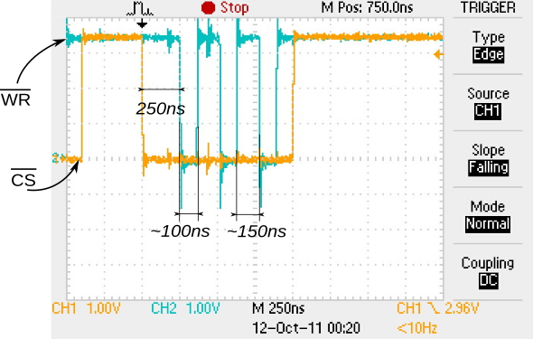
As we’ve seen, it is possible for the processor to perform other duties but it can’t operate on that same port again, so the second order gets delayed until the first one can finish, what gives a period of eight cycles (∼ 100ns), as we can see on the figure, a capture taken during the development phase of a color display driver:
Another possibility is that the AHB bus internal structure allows pipelining succesive requests, this can help to reduce some cycles from the total time.
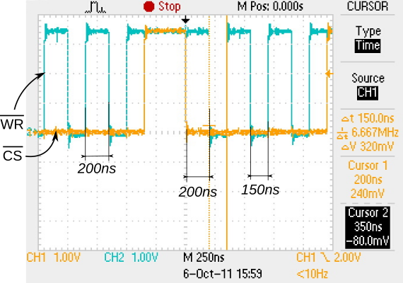
For example, for the TMPM330 from Toshiba, another Cortex-M3, the AHB bus clock and the APB bus clock are user configurable up to a maximum of 40MHz, and also the default value. This processor seems to have some form of pipelining in its AHB bus implementation, ’cause in the very same application we’ve observed a minimum period of six clock cycles (150ns), as can be seen in the following figure:
Up to here, everything is also valid for Cortex-M4 and Cortex-M0 processors.
The Cortex-M0+ processor can optionally have a Single-cycle I/O peripheral connected to its Bus Matrix, which, as its name suggests, allows performing input and output operations in just one cycle. That peripheral is memory mapped and can be accessed using regular data transfer instructions, but these are executed in one cycle instead of two cycles.
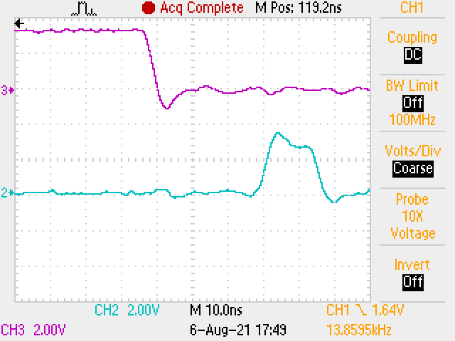
The next figure shows flipping a couple of GPIO pins on an STM32G071 running at 64MHz. The lower trace shows succesive set and reset operations in around 15ns:
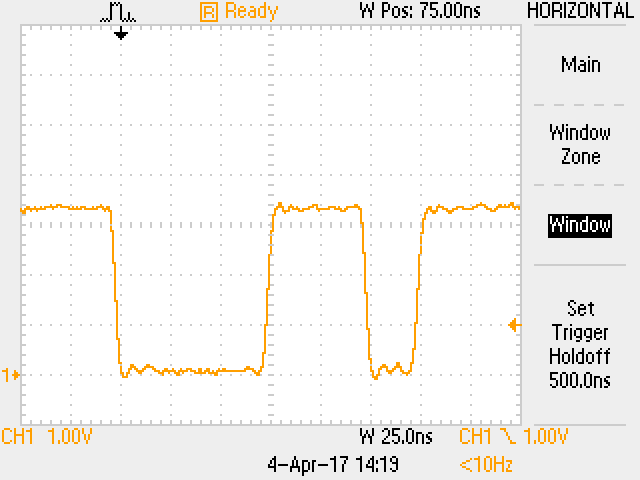
Regarding the I/O management process, and given that to operate on a pin we need to copy the required content from a register to memory, the actual operation in a single cycle would be limited to those cases in which it is possible to keep each required value in its own register and then use only memory transfer instructions in a row. The next capture shows the results of executing two successive read-modify-write operations, followed by two write operations, inside a loop (so we can easily see it), on a Holtek HT32F52231, a 40MHz Cortex-M0+. The first signal reset, at trigger time, includes the time needed to setup all necessary registers; so the time the signal stays in the high state is considerably longer. The first set can then be executed in three cycles (read, modify, write). The second reset takes two cycles (register load, write), while the next set can be executed in one cycle due to the optimizer being able to reuse one of the previously loaded registers:
This post contains excerpts from the book “Desarrollo con microcontroladores ARM Cortex-M3“, taken and translated with the author’s premission.